* This next part of the tutorial assumes that you have completed all the steps in the previous sections
One of Entering the Schematic using a local CIS database, or Entering the Schematic using online component sources, or Entering the Schematic using generic libraries and, optionally, Simulating the headphone circuit with PSpice.
Physical Layout with OrCAD X PCB Editor
After you have completed your design, it is recommended that you run a design rule check (DRC) to isolate any unwanted design errors that might be there. To run a DRC on the headphone design, complete the following steps:
1. In the Project Manager pane select the design file headphone.dsn.
2. From the PCB menu select Design Rules Check
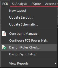
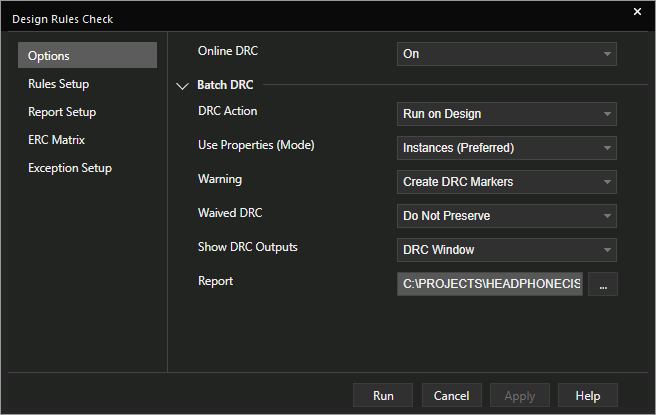
3. In the Design Rule Check dialog box, check Options for DRC Action, Run on Design.
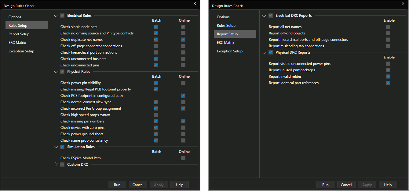
4. Left-click the Rules Setup and Report Setup on the left to view the settings.
5. To run the DRC, left-click>Run.
The DRC report is generated. To view you can either look at the Session log or access the report from the Outputs folder of the Project Manager pane.
Note that a DRC Warning will be flagged for the PARAM part in the Schematic. As this part has no Pins, the "Check device with zero pins" batch DRC option gets this warning issued. This DRC Warning can be ignored as it won't have any impact on any subsequent steps
OrCAD X PCB Editor initial configuration when using footprints from the download data
Start PCB Editor 24.1 from the Cadence OrCAD X and Allegro X 24.1 Windows Start Menu group. If you see Cadence Product Choices, pick any license and left-click>OK. Go to Setup>User Preferences. In the Paths / Library section, left-click the ... for the psmpath entry and use the “+” icon to add a new entry and left-click the “…” button to browse to the location of the symbols folder that the downloaded data was saved to. Left-click>Choose and use the “up arrow” to move that location to the top of the list and left-click>OK.
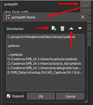
Repeat the steps to add that location to the Paths / Library / padpath preference. Left-click>OK to close the User Preferences Editor and left-click>File>Exit to close OrCAD X PCB Editor for now.
(This isn’t required for the online component sources, or using the generic libraries from the installation, as the path values are set by default.)
Creating the initial board from OrCAD Capture CIS
If not already open, start OrCAD Capture CIS and open the headphone design.
In the Project Manager pane select the design file entry headphone.dsn.
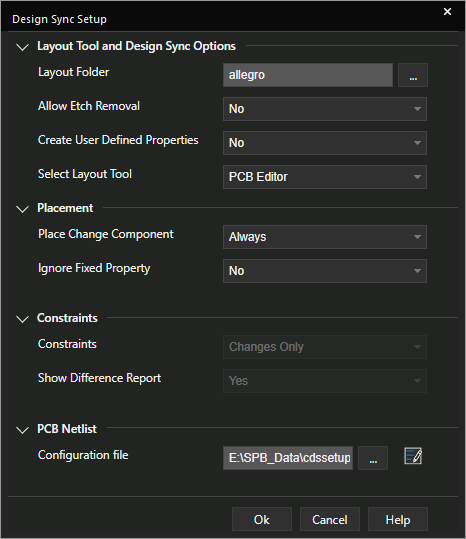
From the PCB menu select Design Sync Setup. Check, or change, the “Select Layout tool” drop-down to PCB Editor and left-click>OK
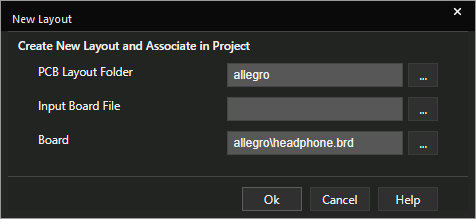
From the PCB menu, select New Layout
Check that the Input Board File is empty to create a board with a default template and left-click>OK
If you see Cadence Product Choices, pick any license and left-click>OK.
The board file, headphone.brd based on a default template, opens in OrCAD PCB Editor
Capture can be closed at this point, "Yes All" to save any changes.
Setting up OrCAD X PCB Editor
These next few steps will guide you through some basic settings inside OrCAD X PCB Editor for this tutorial.
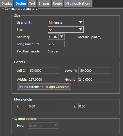
Take Setup>Design Parameters and left-click the Design tab. Check / change the User units drop down to Millimeter, OK any accuracy messages, and check / change the Size to A4. Then check / change both the Left X and Lower Y to -50. (This will move the drawing origin away from the lower left corner of the specified page size.). Leave the other parameters and left-click>OK to accept the changes to the Design Parameters.
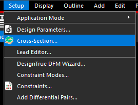
Use Setup>Cross Section from the menu to open the cross section editor.
Here is the initial cross section and default material parameters:

To illustrate changing the cross section, the Conductor material will be changed to Half Oz Copper. Left-click in the Material cell for each conductor layer and select the Half Oz Copper material.

The Thickness and Tolerance will be filled in from the materials settings. Left-click in the Thickness Value cell for the Dielectric layer to get to a total of 1.62mm for the board thickness. That's 1.58444mm in this case.

Left-click>OK to close the cross section editor and accept the changes.
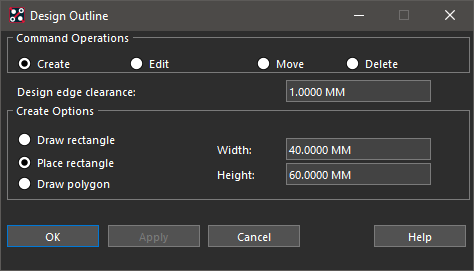
Then take Outline>Design, set the Design edge clearance to 1.0, set the Width to 40 and the Height to 50, then move the mouse from the Design Outline form and the outline will be attached to the cursor. Move the mouse to the Command prompt, left-click in the command prompt, type x 0 0 and press Enter. (This will place the design outline at the drawing origin.) Left-click>OK in the Design Outline form to accept the changes. (The Design Outline will be placed with the Package and Route Keepins 1mm inside it.)
Use File>Save to save, and overwrite, the board at this point
This tutorial uses a simple rectangle for the Design Outline which defines the boundary of the PCB. This can be used for ECAD-MCAD Transfer using DXF, IDX and MCADX as well as manufacturing data.
Use Display>Zoom>Zoom Fit to fit the Design Outline to the canvas
If required, you can adjust the colours of the layers (called Classes and Subclasses). To do this take Setup>Colors from the main menu. The Design Outline is in the Geometry section under Board. Left-click on a square in the Available Colors section and then left-click on the colour square for the subclass entry to set. Left-click>OK to close the colour setup. This method can be used to change any other colours.
Adding Mounting Holes
Now that we have a board outline, let's add some mounting holes to the PCB.
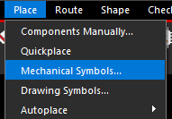
1. Place>Mechanical Symbols. You will see a list of default Mechanical Symbols to choose from.
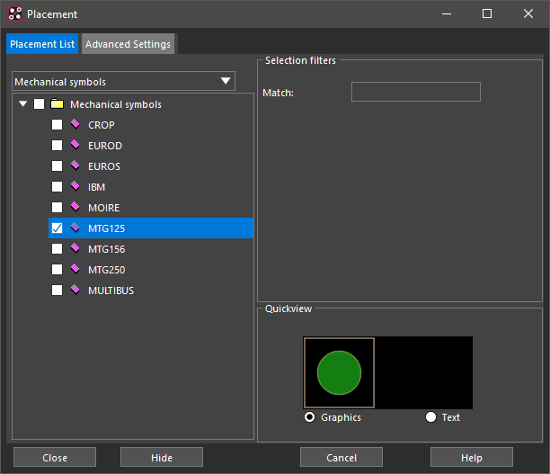
2. Select the MTG125 from the list and place 4 of these on the canvas with left-clicks, selecting the MTG125 each time. Left-click>Close to close the Placement form.
3. Hover the mouse over one of the placed mounting holes and right-click>Move, then move to the Command prompt and type x 3.5 3.5 and press Enter. Repeat the "move" steps and place the remaining mounting holes at x 3.5 46.5, x 36.5 3.5 and x 36.5 46.5.
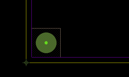
(The placed mounting holes could be fixed by selecting them and taking right-click>Fix with the Symbol active.)
4. Use File>Save to save the board.
Assigning colours to identify Nets
To aid placement and routing, Nets can have colours assigned.
1. Take Setup>Colors, left-click on the Nets tab. Left-click a square in Available colours and left-click the square for Net and the 0 entry to assign the colour, green in this case. (Note that the Net Name may be GND if the PSpice simulation setup steps weren't taken when creating the schematic)
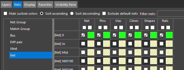
2. Repeat the previous steps to assign colours to the Mid, blue was used for this, and Vpp, yellow was used for this, Nets. Use other colours if you prefer.
Placing Components.
After you have created the board outline, placed the mounting holes and assigned Net colours you can start to place the components in the board. OrCAD X PCB Editor supports both manual and automatic placements. For manual placement you can place parts: from the schematic one part at a time; from the Place>Components Manually list; or by importing the placement.
In this section, start with manual placement from the Place>Components Manually list to create the PCB for the headphone design.
1. For this example, use Setup>Grids and set the Non-Etch grids to 0.5 and the All Etch grids to 0.1.
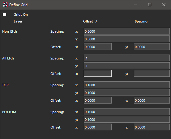
If required, Alignment Guides can be enabled through Setup>User Preferences, Display, Align Guides, Enable Dynamic Alignment
2. To access component placement, use Place>Components Manually. This will display a list of components to be placed. Enable the box to the left of the RefDes to select the component, or components, to place. Move the mouse into the PCB Editor canvas to have the component attached to the cursor, left-click to place the component.
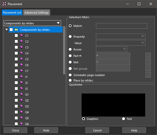
Since there aren't many components to place in this case, an alternative is to use Place>Quickplace to quickly "dump" the parts on the canvas and then move the parts from there. Use the settings in the image below and left-click>Place to place the components from the Quickplace form.
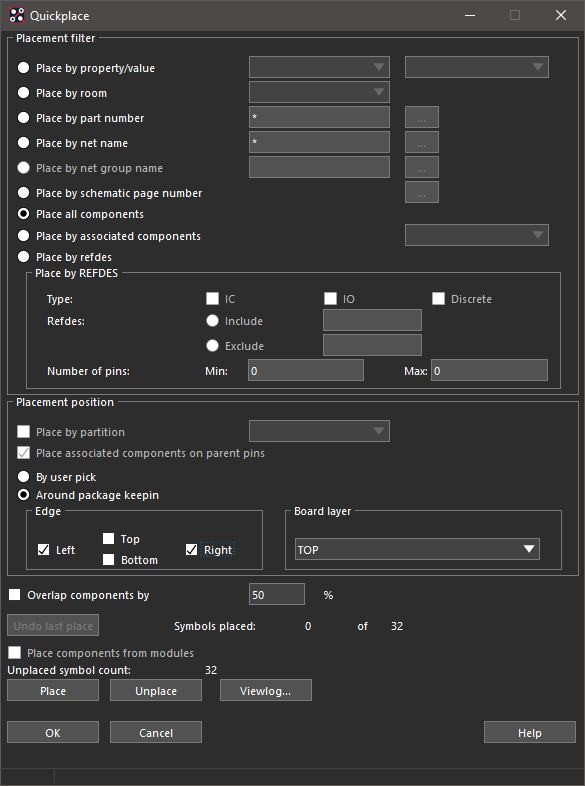
Once placed, using Setup>Application Mode>Placement Edit will favour placement and a left-click on a placed component will attach that component to the mouse cursor for moving and placing. While a component is attached to the cursor, use right-click>Rotate to activate rotate.
See this shot of a sample placement. (Note that your Reference Designators may differ depending on the schematic entry session followed)
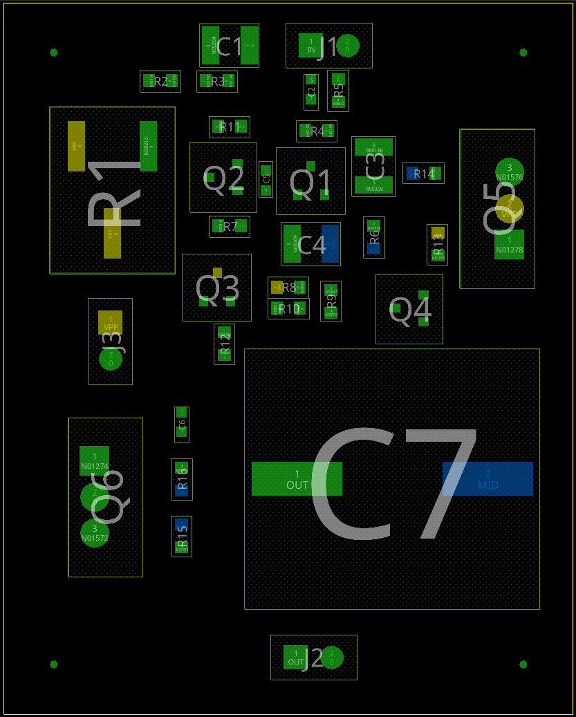
The components with Pins connected to the Vpp Net are roughly grouped around the centre of the board so that a Shape can be used to connect them in later steps.
(Feel free to experiment with placing from the Schematic which require both OrCAD X Capture and OrCAD X PCB Editor running side by side. With Placement active, left-click a component in the Capture Schematic and it will be attached to the cursor when moving to the OrCAD X PCB Editor canvas.)
If you are using the online component sources, you may find that the footprints are somewhat larger than the footprints used for the CIS database approach. Select the Shapes for the Design Outline and Keepins and drag the corners, or vertices, to enlarge the board area, as necessary, to ease the placement process.
Tip: To Find a component in OrCAD X PCB Editor: activate Find, check that Symbols are enabled in the list, type the required RefDes into the Find By Name box and then press Tab, or Enter.
Design Rule Checking
OrCAD X PCB Editor maintains DRC while making changes to the board, use Check>Status to see the current status of the design. Note that Update Shapes followed by an Update DRCs may be required to get the current DRC status. Use the raised buttons for quick reporting from the Status display, "Unplaced Components" for example.
Setting the Design Constraints
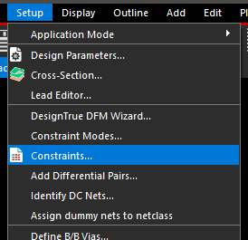
To configure the basic spacing and physical constraints for your board design, select Setup>Constraints. A window appears showing the default settings. For this tutorial, rules will be configured for “default” and “power” Nets.
1. Use Setup>Constraints to launch Constraint Manager.
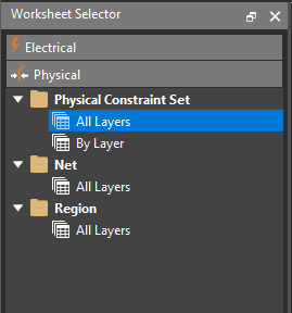
2. Left-click Physical on the left.
3. Left-click in Physical Constraint Set, All Layers
4. Change the value for the DEFAULT rule for Min in Line Width to 0.25
5. Change the value for the DEFAULT rule for Min in Neck Width to 0.25

6. Left-click in the Via cell for the DEFAULT rule. In Filter by Name type via to filter the via names. Double-click VIA-0_5-0_2 from the list to add to the Via List. Select the default VIA entry in the Via List pane and left-click>Remove. (or double-click the entry to remove it) Then left-click>OK to set the Vias in the design.
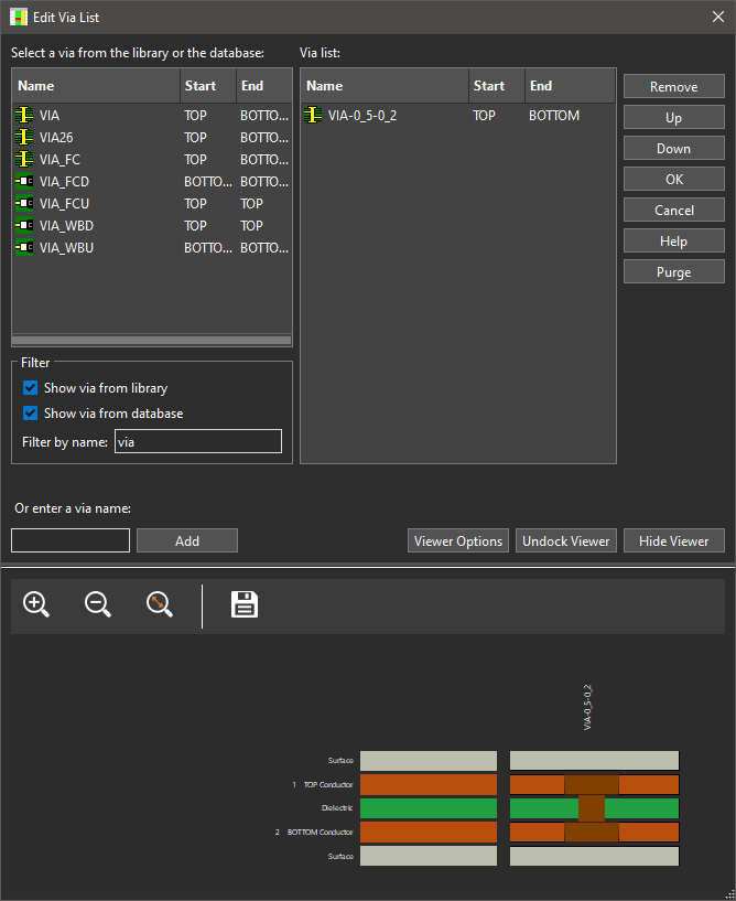
(The required VIA-0_5-0_2 is in the downloaded data. Leave the VIA entry, which will be a larger via, if not using the downloaded data)
7. Right-click in the DEFAULT cell and take Create>Physical CSet, name the new CSet power (This will be converted to uppercase after the OK) and left-click>OK

8. Change the value for the POWER rule for Min in Line Width to 0.5

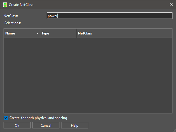
9. Move to Net, All Layers. Right-click in the Headphone cell and take Create>Class, name the new Class Power and ensure that Create for both physical and spacing is enabled.
10. Locate the 0 Net in the list and use right-click>Add to>Class select POWER from the drop-down at the top and left-click>OK to add the Net to the Class.
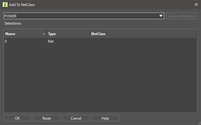
11. Repeat the previous step to add the VPP Net to the POWER Class.
12. In the POWER Class, left-click in the Referenced CSet cell and select POWER from the drop-down.
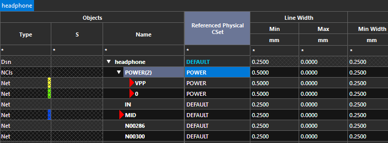
13. Now move to Spacing on the left with a left-click.
14. Left-click, Spacing Constraint Set, All Layers
15. Left-click in the Line To cell for DEFAULT, ensure that the cell is selected and not the value, then drag the mouse to the Bond Finger To cell to select the row. The Bond Finger To cell will be opened for editing, change the value to 0.25 and press Tab, or Enter, to set the values.

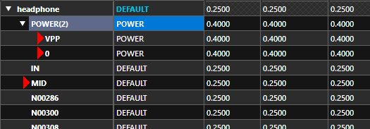
16. Right-click in the DEFAULT cell and take Create>Spacing CSet, name the new CSet POWER and repeat the previous step to set the values to 0.4

17, Move to Net, All Layers and left-click in the Referenced CSet cell for the POWER Class and select POWER from the drop-down.
Routing
After completing the board placement, you can route the headphone board to complete the electrical connections between components.
OrCAD X PCB Editor supports manual or assisted routing. For this tutorial, manual routing will be used.
The basic steps involved in the manual routing process are as follows:
Check the board outline, via definitions, routing and via grids.
Route power and ground
Fan out surface mounted devices and verify connections to power and ground.
Route the remaining signals using the manual routing tools.
Optimise routing using the manual routing commands.
Check for route spacing violations and check routing statistics.
Connecting VPP and GND (0) nets
For this tutorial, these Nets are going to be, primarily, connected by Shapes on the Bottom Layer.
1. Take Setup>Colors, left-click>Off for Global Visibility. In the Stack-up group, left-click the All square for Bottom, left-click the Pin square for Top.

Move to the Geometry group and left-click the square for Design_Outline to make that visible.
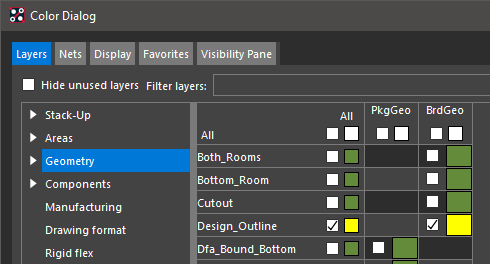
Left-click on the Areas group and enable the All visibility of both Pkg KI and Rte KI.

Then left-click>OK to close the Color Dialog.
2. Take Shape>Polygon from the menu.
3. In Options, set the Active Class and Subclass for the Shape to be Etch and Bottom using the drop-downs. Left-click the ... button for Assign Net Name and double-click the Vpp entry. Left-click in the Type for Segment Type and pick Line Orthogonal.
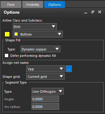
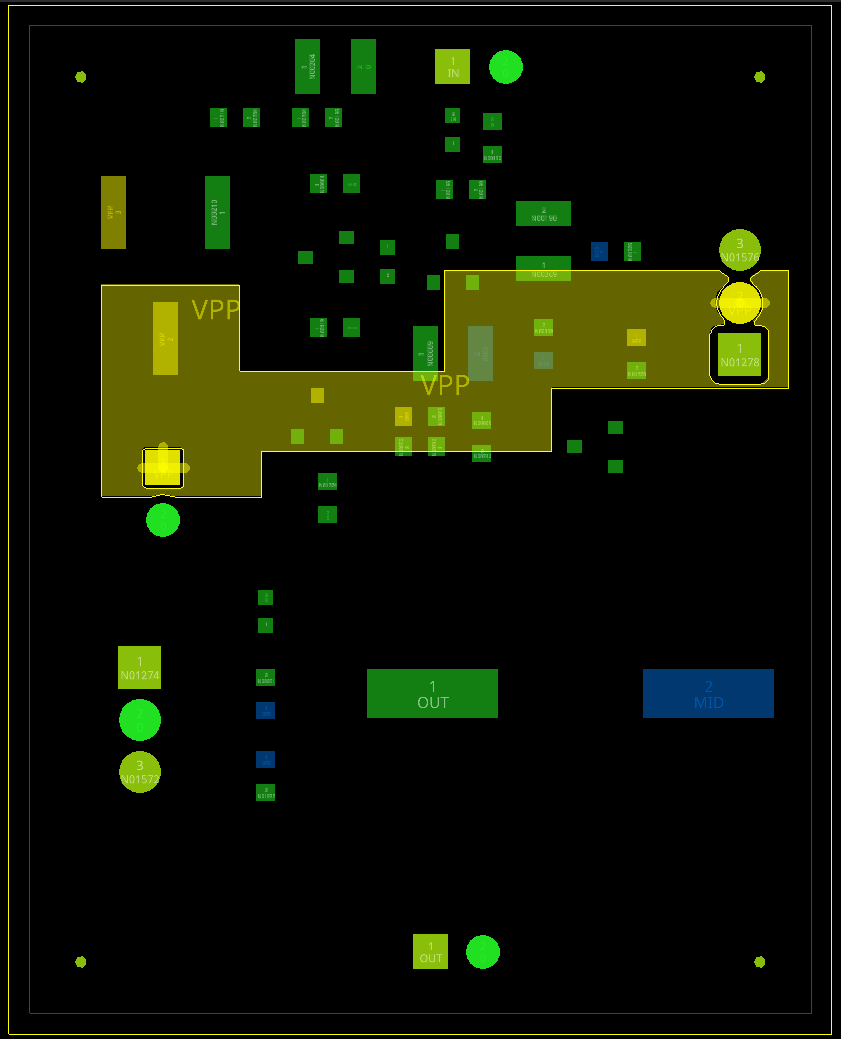
4. Move to the canvas and use a left-click to start adding the Shape around the yellow, coloured, Vpp Pins, use left-clicks to add corners to the Shape as it is added. Note that the Shape Boundary may not cross itself and that the Shape being added will always be "closed" back to the initial point that the Shape was started from. Right-click>Complete to finish the Shape without needing an exact click on the starting point. The Shape can still be edited at this point using the corners and vertices. Use right-click>Done to end adding the Shape.
5. Use Setup>Application Mode>Shape Edit to favour Shape Editing. In Options, check that the Active Class and Subclass are set to Etch and Bottom, set the Corners to Round and the Radius to 0.5.
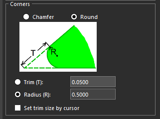
Move to the canvas and select the Vpp Shape with a left-click, then right-click>Trim Corners.

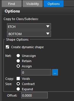
5. Use Setup>Application Mode>General Edit to revert to general editing. Then Shape>Z-Copy from the menu. In Options, set the Copy To Class / Subclass to Etch and Bottom, enable Create Dynamic Shape, set the Net to Assign, use the ... under assign to browse the Nets, and double-click the 0 entry to assign the Net. Move to the canvas and left-click the Keepin In boundary to create the Shape.
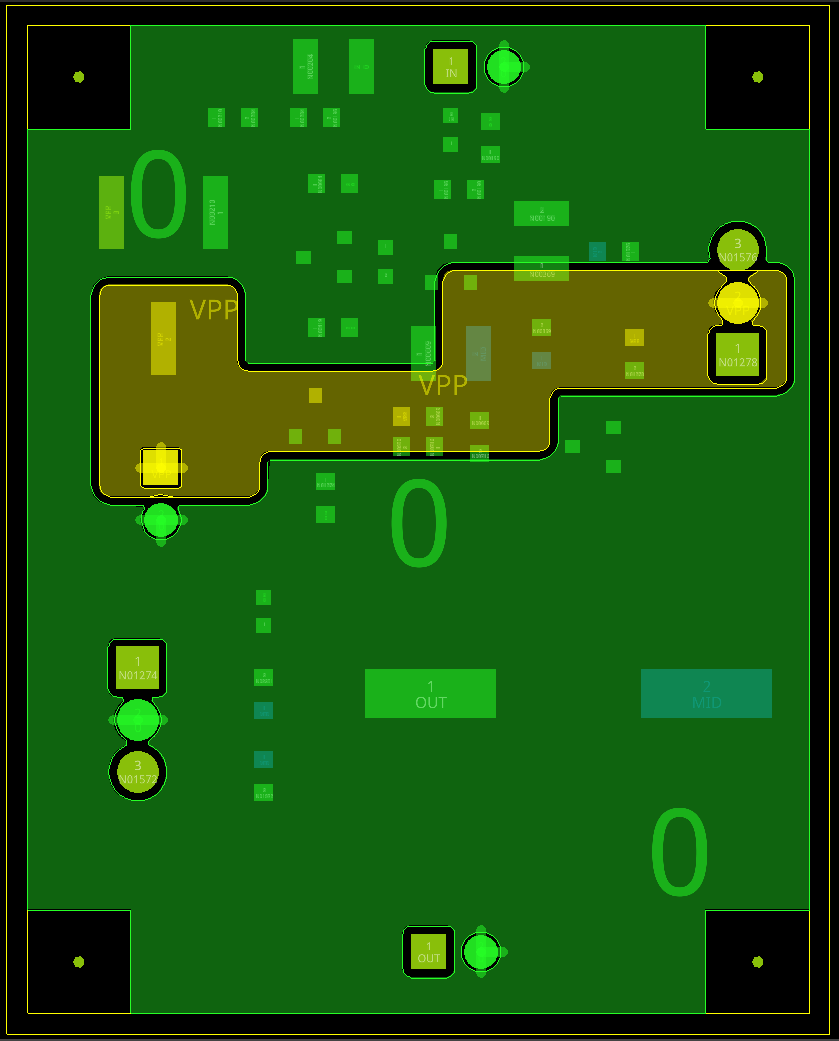
The Vpp Shape will be cleared from the added 0 Shape. If that isn’t the case, use Shape>Select Shape or Isolation / Cavity, hover the mouse over the a Shape and select Raise Priority, or Lower Priority.
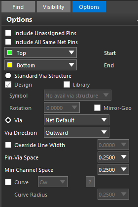
6. Select Route>Create Fanout from the menu. In Options, set Start / End to Top / Bottom, and set Via Direction to Outward.
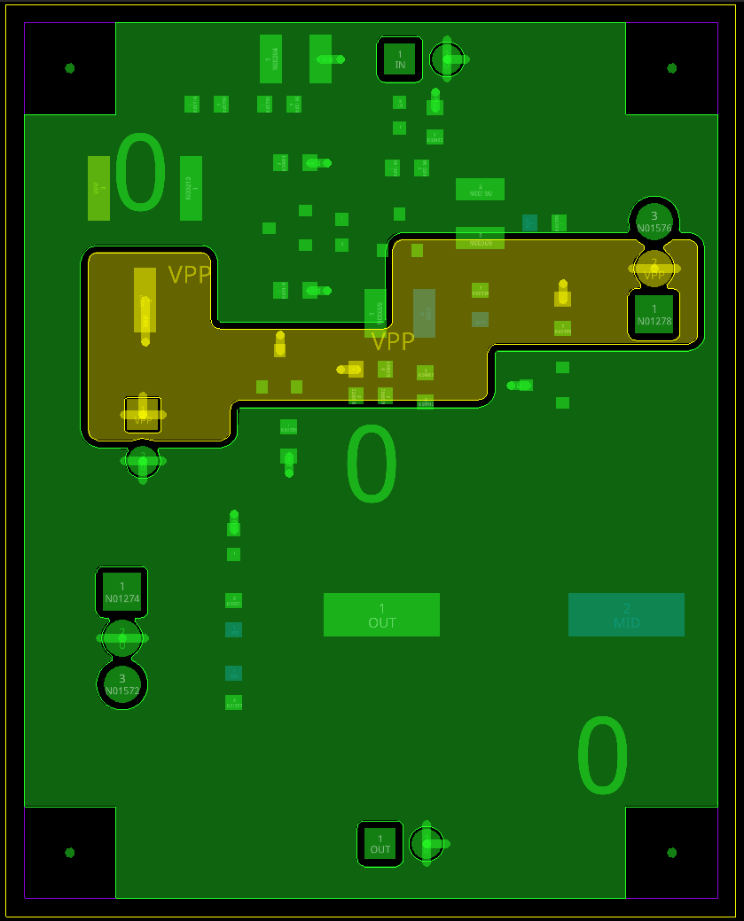
In Find check that only Pins are enabled. Work through the Pins for the 0 and Vpp Nets, left-clicking on the Pins to add the fanout. Right-click>Done to end adding the fanout.
Connecting the “other” Nets
1. Go to Setup>Colors and, in Stack-up, turn off all the Bottom objects and turn on all the Top objects.
2. Use Route>Connect to initiate routing. Check Options for Top / Bottom being the layer selections and Line Lock is set to Line / 45. Also check that Find has, at least, Pins enabled.
3. Left-click on a Pin to start adding a connection. Left-click to accept what is routed and, potentially, add a corner. Left-click on the target Pin to complete the route. Double-click while routing to add a Via
You could simply left-click on Pins to make the connections and then revise the routing or you could more carefully add the routing avoiding conflicts.
In any case, you may need to delete and reroute some of the connections. Trace Segments and / or Traces will need to be enabled in the Properties panel Selection Filter pane. Select a Trace, or Trace Segment and right-click>Delete, to delete the selected item.
To Slide a routed connection, ensure that, at least, CLine Segs are enabled in Find and then left-click and drag on a CLine Segment to move the connection.
You may also find that, as routing is added, revision to placement is required.
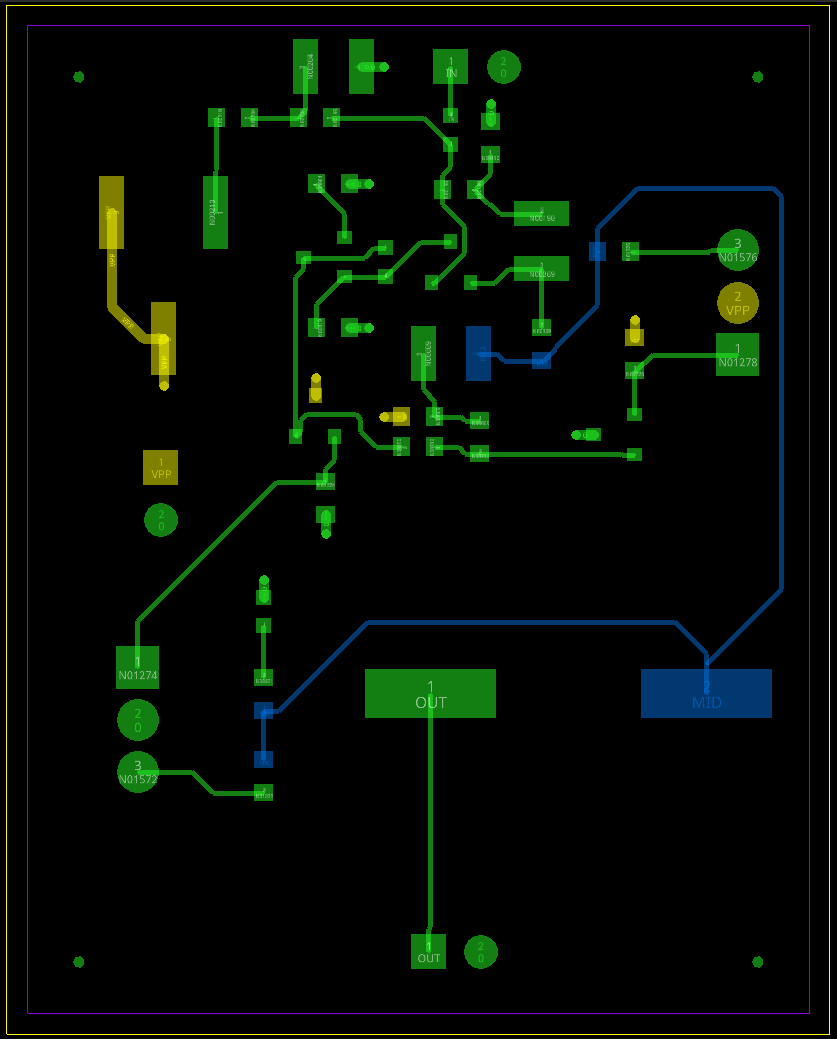
Once you are happy with the placement and routing, move onto the next steps.
Generating output
Nothing gets manufactured without manufacturing data. OrCAD X PCB Editor generates Gerber, IPC-2581 and, with the third-party ODB++ Inside application is installed, ODB++ format.. For this example, Gerber (Artwork) and drill (NC) data will be generated. the data that gets exported for manufacturing is controlled by the configured Films.
1. From the main menu, take Export>Gerber
2. Left-click the General Parameters tab in the Artwork Control Form and check that the Device Type is Gerber RS274X and that Integer places is set to 2 and Decimal places is set to 5.
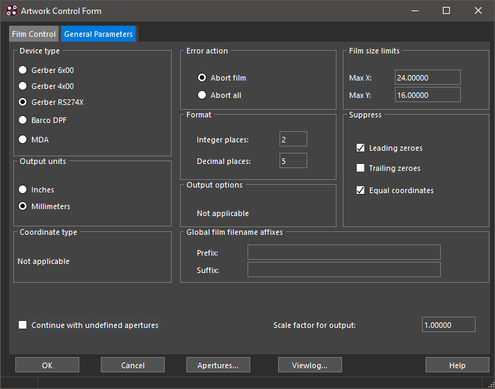
3. Move back to the Film Control tab. Note that the Films for the Etch (routing) Layers, Top and Bottom, are automatically added.
Typically, the manufacturing output will contain more than just the Etch layers. For this example, the Config will be used to automatically create some typical additional Films.
4. Left-click>Config... on the Film Control form.

The Artwork Configuration form is displayed. For this example, the defaults will be fine, so scroll through if you want to examine the values and left-click>OK to accept the defaults.
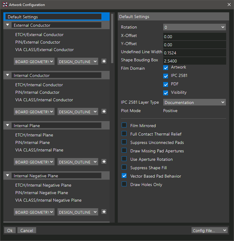
Left-click>Yes on the message about the regenerating the Film records and the additional Films will be added to the Film Control form.
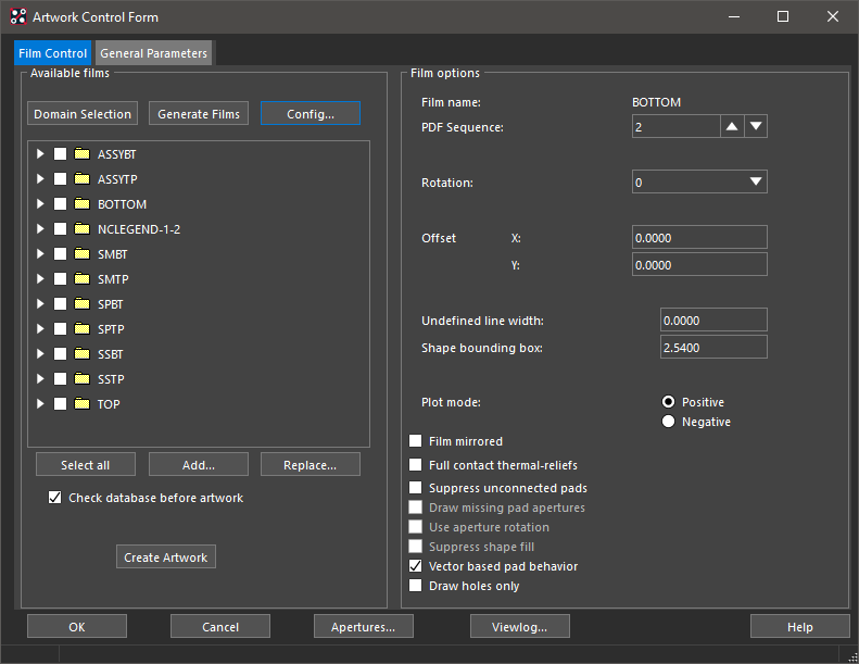
Left-click>Select all to create all of the Films and left-click>Create Artwork to create the Gerber data.
In the "view of file: photoplot" window that opens, there will be warnings about not having a Photoplot Outline defined and using the Undefined Line Width for some objects. These warnings can be safely ignored and the "view of file: photoplot" window can be closed.
Left-click>OK to close the Artwork Control form.
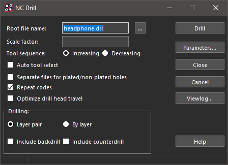
Left-click>Export>NC Drill, the default settings should be fine so, left-click>Drill to create the drill data. Then left-click>Close to close the NC Drill form.
There are numerous reports from PCB Editor. For this example, take Export>Quick Reports and select the Summary Drawing Report from the list.. Look through the created report and then close the report viewer window.
Viewing the completed board in 3D
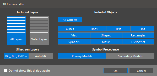
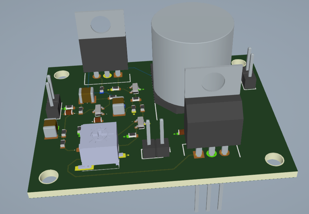
Go to Display>3D Canvas, check that All Objects are enabled and left-click>OK to build the 3D view and open the 3D Canvas. If the provided footprint library was used, the footprints within that will have 3D models mapped and the board will be seen with the assigned 3D models.
Roll the mouse wheel to Zoom., control+middle mouse click to Pan and shift+middle mouse click to Rotate.
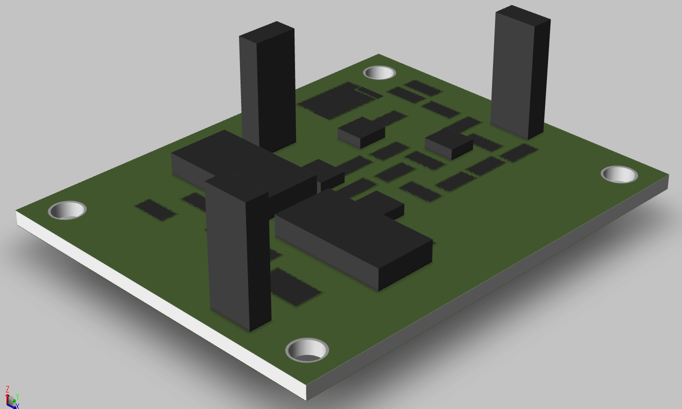
The generic libraries don't have any 3D models provided but the 3D models from the "stepGeneric" folder of the downloaded data could be mapped. The footprints from the online sources may have 3D models as part of the download for the selected parts but, typically, they won't be mapped.
The image below is from an example placement of the components using the generic libraries. This is only using the Place Boundaries and assigned heights so the display has no model details.
To illustrate the 3D model assignment, the parts from the board using the generic libraries will be mapped to a 3D model from the downloaded data
In the 3D Canvas view, left-click the 3D Mapper tab to get the 3D Model Mapper active. At the right, the Models and mapping for the footprints in the design will be shown
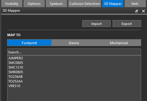
Left-click one of the footprint entries to see the footprint(s) highlighted in the canvas. The lower section of the 3D Mapper tab, the ... button for Model File will allow browsing for the 3D Model to assign. In this first case, the Jumper2 STEP Model is assigned and mapped correctly, that isn't always the case as following examples will show.
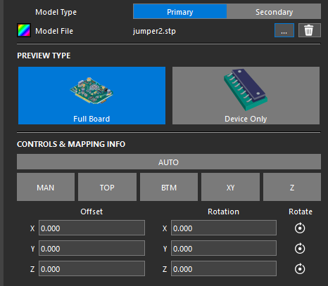
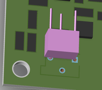
Next the 3D Model for the VRES10 will be mapped. Follow the previous steps to get the VRES10 STEP Model assigned. It's clear from the 3D view that the mapping is incorrect.
Change the mapping option from Full Board to Device Only. This will display just the specific model to be mapped and make mapping much easier
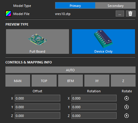
Left-click the Auto button in the mapping options to see if the mapper can work out the mapping from the component and 3D Model. That doesn't work well in this case so some more mapping will be required. Manipulate the 3D view using the middle mouse controls above so that the bottom face of the 3D model is in view. Left-click the Top button in the mapping options and hover the mouse over the bottom face of the 3D model and left-click.
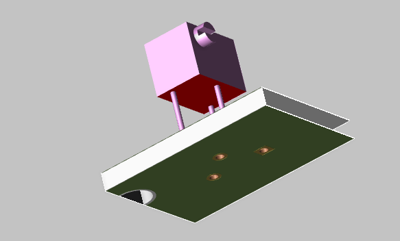
That is looking better, in that the face gets mapped but the mapping still isn't ideal as the Pins aren't aligned.
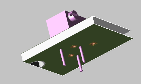
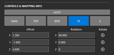
There are a couple of ways to fix this. Firstly with the XY: The XY function may need the rotation set before the mapping can be completed so, in this case, set the Z rotation to 0, then left-click the XY button in the 3D Mapper.
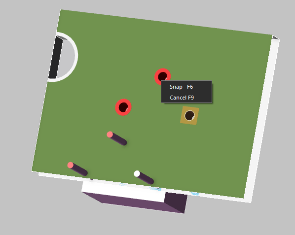
Use the middle mouse controls to get to the bottom view of the Pins and board. Left-click the "head" of two of the Pins.
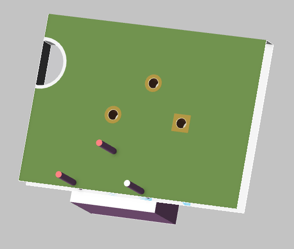
Left-click on the two holes that the Pin will mount through and right-click>Snap.
After the "snap" has happened, the Pins and Holes will be aligned.
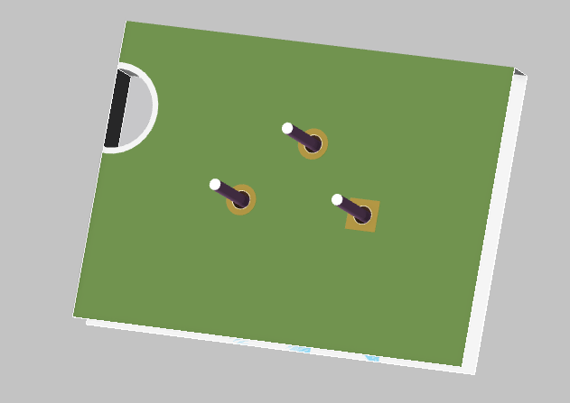
The XY and "snap" works well for through pins since there is a clearly defined location for the Pin. This doesn't usually work as well for surface mount pins as the pads are larger and there isn't such a clearly defined location. The other method is to use manual alignment. Left-click the Man(ual) button in the 3D mapper.
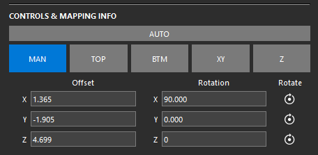
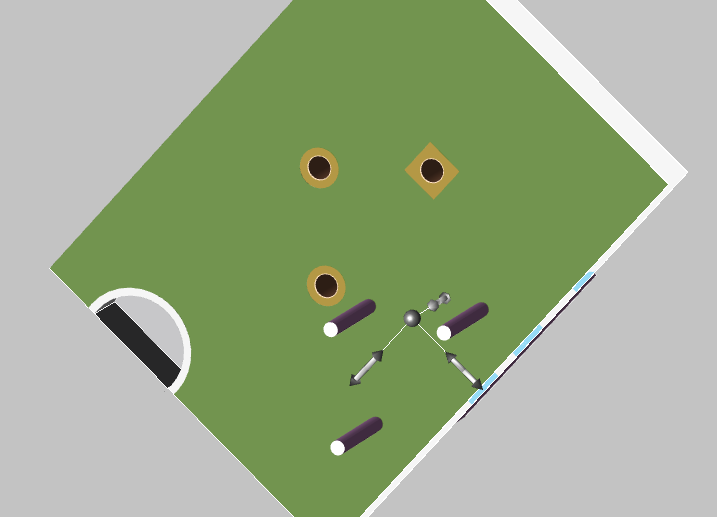
This will activate the 3D axis on the part so that a left-click and drag on an axis will move the 3D model along that axis. The middle mouse controls can be used to maipulate the view of the model to check that the mapping is accurate.
The next image shows the final mapping parameters for the VRES10 footprint.
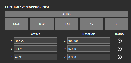
Here are the mapping parameters for the remaining generic parts
| Footprint: | smc0805 | ||
|---|---|---|---|
| X: | 0.9995 | Rot: | 0.0 |
| Y: | 0.0025 | Rot: | 0.0 |
| Z: | 0.6000 | Rot: | 0.0 |
| Footprint: | smc1210 | ||
| X: | 1.6767 | Rot: | 90.0 |
| Y: | 0.0025 | Rot: | 0.0 |
| Z: | 0.5750 | Rot: | 0.0 |
| Footprint: | smr0805 | ||
| X: | 1.1672 | Rot: | 0.0 |
| Y: | 0.6226 | Rot: | 0.0 |
| Z: | 0.0000 | Rot: | 0.0 |
| Footprint: | to236ab | ||
| X: | -1.0414 | Rot: | 0.0 |
| Y: | 1.0287 | Rot: | 0.0 |
| Z: | 0.0000 | Rot: | 180.0 |
| Footprint: | to252aa5 | ||
| X: | 2.3868 | Rot: | 90.0 |
| Y: | 4.9797 | Rot: | 0.0 |
| Z: | 0.0000 | Rot: | 0.0 |
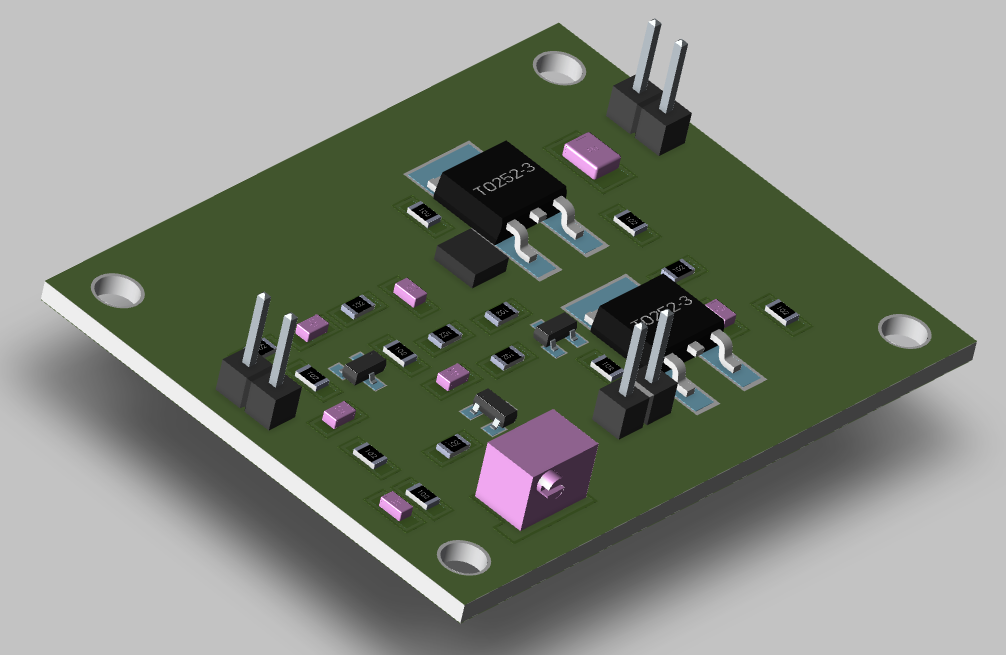
The next image shows the 3D view after all the 3D models have been assigned and mapped.
Copyright © 2025, Parallel Systems Ltd.
All rights reserved.
