Entering the Schematic using online component sources
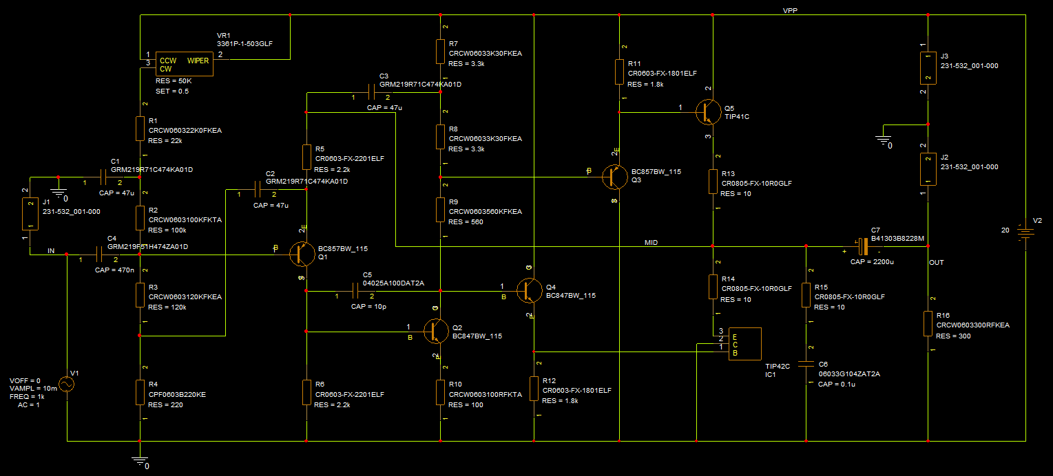
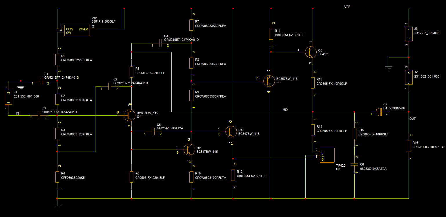
Completed schematic using suggested parts with PSpice Models assigned
Note that online component resources do not contain the properties required for PSpice simulation so the downloaded data contains a sample library of PSpice models that can be associated with components from online sources to facilitate simulation with PSpice.
The online component resources have several sources available and different components may be available from different sources. The advantage of the online component sources is that no library development is needed, the disadvantage is that, whilst the downloaded components are completely satisfactory for designing products, they may not meet required internal standards.
This tutorial is going to use components from SamacSys but the other online component sources could be used.
Starting the Project
Begin by starting OrCAD Capture CIS 24.1 using any license. If prompted, log into Cadence using your Cadence Support credentials, or OK the license message if you don’t have any cloud access enabled. Then, in the opened Capture application, use File>New Project to start a New Project, name the project Headphone, for example. Check the Enable PSpice Simulation if the design is to be simulated with PSpice (essential!), leave this unchecked if there isn’t a PSpice license available, and simulation isn’t required. Specify a folder for the project location. The Use Workspace is optional but will fix the project location.
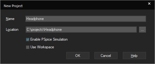
If Enable PSpice Simulation was checked, base the new project on the empty.opj existing project when prompted for a project template. If prompted, confirm the PSpice license to be used for this session.
Initial setup
Left-click on the "+" for headphone.dsn, then the "+" for SCHEMATIC1 and double-click on the PAGE1 entry to open the Page. Once the Page is open, right-click on the PAGE1 entry and take Schematic Page Properties.

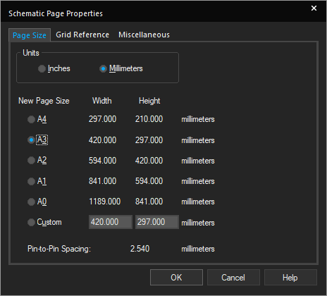
In the Page Size tab, set the Units to Millimeters, select the A3 entry and left-click>OK to change the Page size. (The online components are a bit larger than the default library parts and there is no need to “squeeze” the Schematic onto a smaller page.)
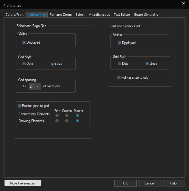
Take Options>Preferences from the main menu and, in the Grid Display tab, set the Grid Spacing to 1 / 2 of Pin to Pin and left-click>OK. (The online components use a smaller grid than the default)
Placing the parts
Double-click on the PAGE1 entry to open the Schematic Page. Left-click in the Schematic Page to activate it and then use Place>Component from the menu. Left-click the SamacSys entry on the left, enter Cadence account credentials, if prompted for them. When the initial list of SamacSys parts has been loaded, use the Search at the top and enter 50k trimmer as the search value. Left-click the 3361P-1-503GLF result to load the part properties on the right and double-click on the selected entry to download the part, generate the data, move to the Schematic Page and place the part. Left-click to place the part in the page.
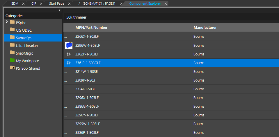
Work through the parts in the following list, the first entry is there for reference. Press the R key with the component on the cursor to Rotate. Either drop the component Pins together and then drag the components apart to add a Wire or use Place>Wire (or the W key), left-click on a Pin to wire the components together, if required, press Esc to end placing a Wire. Connecting the parts as you go is probably best as the value of the component will be in the search, but the placed component will be showing the Part Number.
(In the list: Search is what to enter in the Place>Component search, note the use of O (capital o) following the value of low value resistors; Pick is the component picked for this example, others could be used but check that both Schematic Part and PCB Footprint are available. STEP (3D) may also be available. The "pick" value in the table could also be used for the Search)
| Search | Pick | Quantity | RefDes |
|---|---|---|---|
| 50k trimmer | 3361P-1-503GLF | 1 | VR1 |
| 22k resistor | CRCW060322K0FKEA | 1 | R1 |
| 100k resistor | CRCW0603100KFKTA | 1 | R2 |
| 120k resistor | CRCW0603120KFKEA | 1 | R3 |
| 220 resistor | CPF0603B220KE | 1 | R4 |
| 2k2 resistor | CR0603-FX-2201ELF | 2 | R5,R6 |
| 3k3 resistor | CRCW06033K30FKEA | 2 | R7,R8 |
| 560 resistor | CRCW0603560KFKEA | 1 | R9 |
| 100O resistor | CRCW0603100RFKTA | 1 | R10 |
| 1k8 resistor | CR0603-FX-1801ELF | 2 | R11,R12 |
| 10O resistor | CR0805-FX-10R0GLF | 3 | R13,R14,R15 |
| 300O resistor | CRCW0603300RFKEA | 1 | R16 |
| bc857 | BC857BW,115 | 2 | Q1,Q3 |
| bc847 | BC847BW,115 | 2 | Q2,Q4 |
| 47u capacitor | GRM219R71C474KA01D | 3 | C1,C2,C3 |
| 470n capacitor | GRM219F51H474ZA01D | 1 | C4 |
| 10p capacitor | 04025A100DAT2A | 1 | C5 |
| 100n capacitor | 06033G104ZAT2A | 1 | C6 |
| tip41 | TIP41C | 1 | Q5 |
| tip42 | TIP42C | 1 | IC1 |
| 2200u capacitor | B41303B8228M | 1 | C7 |
| header 2 way th | 231-532/001-000 | 3 | J1,J2,J3 |
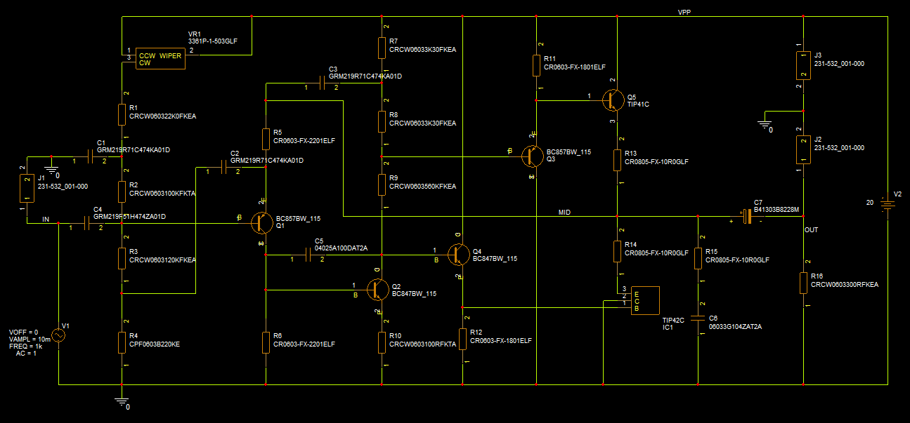
Use the completed schematic above (and below) for reference as you enter the schematic. The exact layout of the schematic is not critical to having a working example but correctly connecting the various elements will be required to get the circuit to work as expected, if simulating. Some of the reference designator prefixes may be different if different components, or components from other sources, have been used.
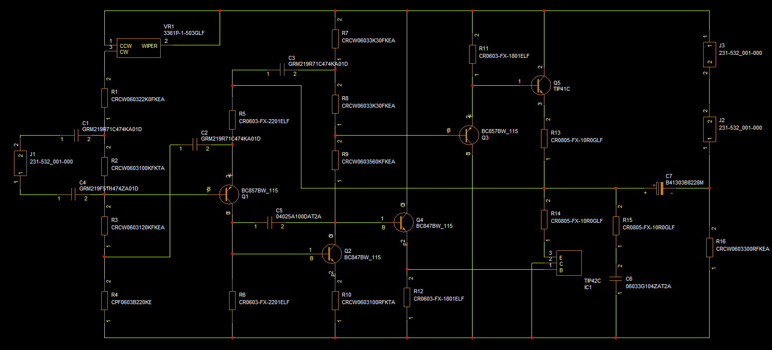
Use File>Save from the menu to save the current schematic.
So far, all the wires have default, system assigned, names, these will be formatted as "N" followed by an identifying number. Whilst these names will work perfectly as far as the design is concerned, it will be much easier to identify key net names if the default net names are overridden with Net Aliases. From the menu, Place>Net Alias (or press the N key), this form will open:
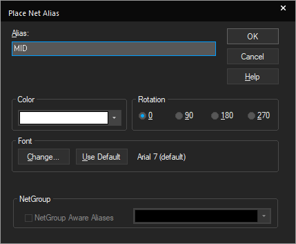
Then type in the required Net Alias name to assign in the Alias field, the value needs to be MID in this case and left-click>OK. The Net Alias value will be attached to the cursor and can be applied to a net by clicking on the net to "stick" the Net Alias to it.
(Some things to note about placing Net Aliases: IF the Net Alias ends in a number, the number will be automatically incremented, so a value of A0 will become A1 and so on, it is not possible to disable this; The Net Alias value will remain on the cursor so that it can be assigned to other wires, note that nets of the same name on the same schematic page will automatically be connected by the netlister so don't "accidentally" apply the same Net Alias to nets that you do not intend to have connected.)
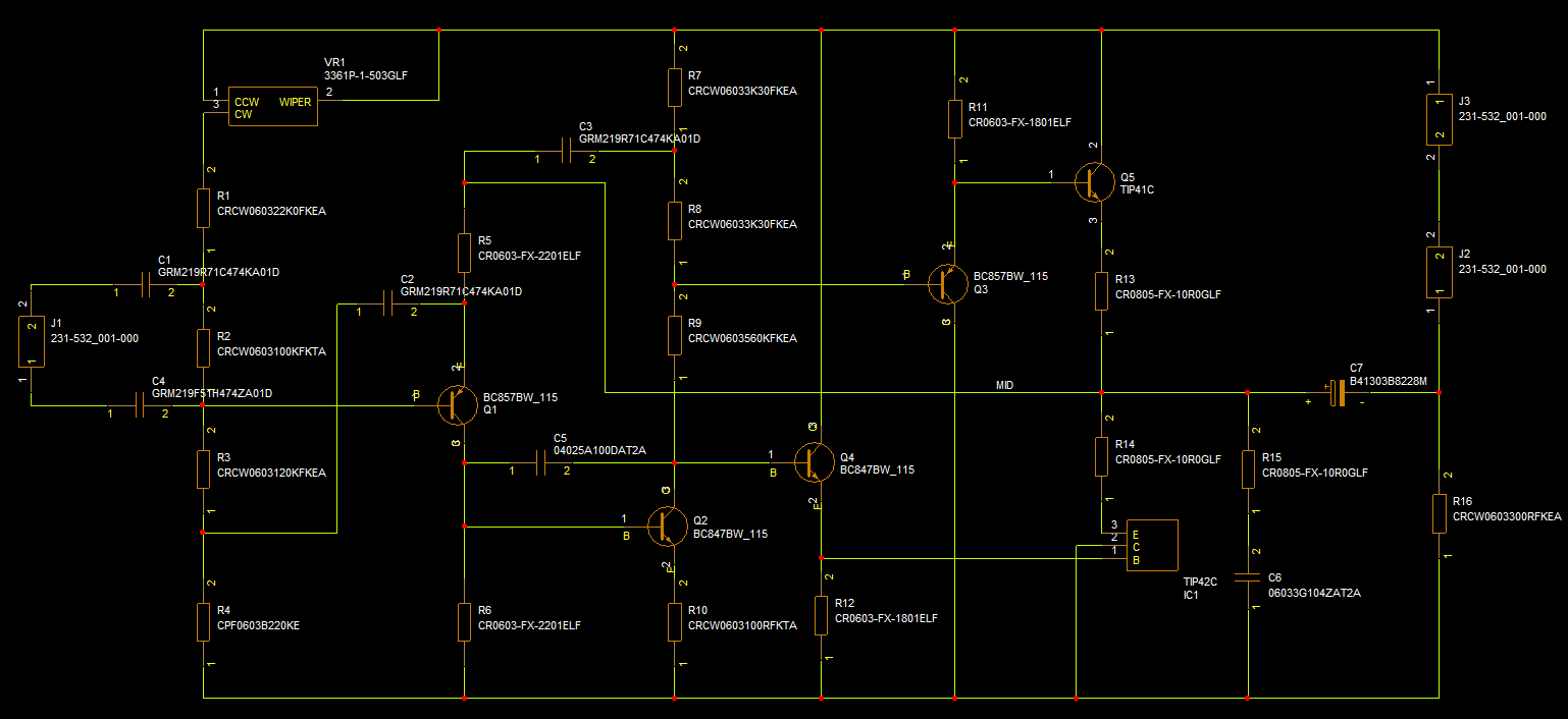
Net Alias "MID" shown assigned to the wire at the junction of the two output transistor emitter resistors.
Use Place>Net Alias again to assign the IN, OUT and VPP Nets Aliases to the wires as shown. When placing the Net Aliases, control+E can be used to change the name on the cursor, rather than using the Place>Net Alias menu / icon three times.
If NOT simulating with PSpice:
Use Place>Ground from the menu to place the GND symbol from the Capsym library for the common Ground connections.
Use File>Save from the menu to save the current schematic.
Either move to the Physical Layout with OrCAD X Presto section. Or move on to the Physical Layout with OrCAD X PCB Editor section.
If simulating with PSpice:
Add the PSpice sources:
Use Place>Component and, in the Component Explorer, left-click on PSpice, use the Search at the top and type VSIN in the Part box, double-click the VSIN result and place the VSIN part in the Schematic as V1. Double-click the placed part and set the properties: VOFF to 0, VAMPL to 10m, FREQ to 1k and AC to 1; for information: this will provide a 10mV sine source at 1kHz for Transient Simulations and a 1V source for AC Sweep simulations, which are covered later. Go back to Place>Component and the PSpice parts, search for VDC and place a VDC part in the Schematic, referenced V2, for the power supply, double-click the displayed value and change 0Vdc to 20 for this circuit, PSpice will "know" that the value is a DC voltage, so it is not necessary to specify V, or Vdc, with the value. Use Place>Ground from the menu to place the 0 symbol required for the PSpice reference, this is from the Capsym library
Use File>Save from the menu to save the current schematic.
Assign the PSpice models
The online component resources don’t have any PSpice properties assigned. Since these properties are essential to simulating, the placed components will be associated with the PSpice models from the downloaded library. The names of the PSpice models start with the circuit value to simplify their selection from the list of models in the library.
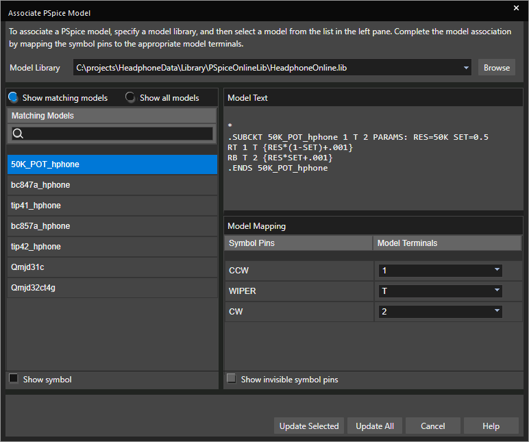
Left-click in the Schematic Page to active it. Move to the “pot”, left-click to select it and right-click>Associate PSpice Model. Use the Browse to the right of Model Library to browse to the location of the downloaded HeadphoneOnline.lib file. The “pot” has three pins so the list contains all the models with three Pins. The 50K_POT_hphone entry should be the selected entry, and is the required model for the “pot”. The text of the model is shown and, currently, the Model Mapping section has no Pins mapped as the Symbol Pin names from the Schematic Part and the Model Terminals from the PSpice Model are not an exact match. In the Model Mapping section, use the drop-down for the CCW Symbol Pin and select 1 in Model Terminals. For the WIPER Symbol Pin, select T as the Model Terminal and for the CW Symbol Pin, select 2 as the Model Terminal. Left-click>Update Selected and left-click>OK to complete the assignment.
Right-click>Edit Properties for the “pot”, left-click on the RES cell and control+left-click on the SET cell and right-click over one of the selected cells and take Display. In the Display options, select the Name and Value option and left-click>OK. Having the RES property visible is helpful for identifying the correct circuit values and having the SET property visible will be convenient later in the PSpice simulation steps.
Work through the remaining components in the Schematic. Except for the output capacitor, the other components should have an automatic assignment between the Symbol Pins and Model Terminals. This isn’t the case for the suggested components but take care to check the correct assignment if the Symbol Pins for a transistor are 1, 2, 3 rather the B, C, E. The suggested output capacitor has Symbol Pins of + / - so map the “+” Symbol Pin to Model Terminal 1 and the “–“ Symbol Pin to Model Terminal 2. (PSpice models aren’t generally polarity sensitive so the simulation will run if the capacitor polarity is reversed.) Again, if a different component was selected the Symbol Pins may also differ.
If you want to have the circuit values visible, the Resistors have a RES property, and the Capacitors have a CAP property that can be made visible.
For reference, the sample References and associated models:

Use File>Save from the menu to save the current schematic.
Now move to the Simulating the headphone circuit with PSpice section.
Copyright © 2025, Parallel Systems Ltd.
All rights reserved.
