OrCAD X and Allegro X PCB Matrix Key: A tick confirms that the feature is included in the suite. An option name  means you need to purchase the option to get the feature included in the suite

Features OrCAD X Standard OrCAD X Professional ALLEGRO X Artist ALLEGRO X Designer ALLEGRO X Designer Plus ALLEGRO X Venture
Floating Networked License
12 Months Maintenance Support Included In Purchase Price
SCHEMATIC ENTRY + DATA MANAGEMENT
Flexible Window layout
Graphical, flat and hierarchical page editor and Picture block hierarchy
OrCAD PSpice AD Basic - Restricted Capacity - see PSpice Matrix below
Net Groups - Complex bus definition
AutoWire
44,000 Schematic symbols
Coloured Components / nets
Tcl TK scripting support
Online design rule check including custom DRC capability and Waive DRC
Forward and back-annotation of properties / pin-and-gate swaps
Schematic Part and Library editor
Cross-probing and cross-placing
FPGA design-in / pin import & export
Multiple PCB netlist interfaces - New Design Sync for Cadence Flow
UltraLibrarian, Samacsys and SnapMagic (Symbol, Footprint 3d Step Model)
Property editor for pins, components, nets
OrCAD SigXplorer SI Analysis
Intelligent PDF creation
Advanced Annotation
Design Compare (detail and Graphical)
Default Demo designs
Extended Preferences
Export ISCF (Intel Schematic Connectivity Format)
Export / Import XML
Altium Importer Schematic (PCB also available)
Eagle Importer Schematic (PCB also available)
Constraint Manager
Ability to create. manage part database schema and libraries in cloud
Manage Virtual team and collaboration workspaces
Ability to share and work collaboratively for libraries and design
OrCAD X Cloud Services 10G 50G 50G 50G 50G 50G
LiveBOM using Datalynq and Sourcengine
Component Information System
Windows ODBC compatible format
Interface to relational database and management systems
Database query for part selection and parametric properties
Schematic and BOM Variants Manager (Parts not Fitted and more).
Component Information Portal (CIP), Access to Mouser, Digikey, Future, Farnell CIP E Option CIP E Option CIP E Option CIP E Option CIP E Option CIP E Option
DE-HDL / System Capture
PCB EDITOR
Markup for design reviews
Spacing, Same net, Netclass and Class to Class rules
Physical Constraint Rules
3D DRC Rules(Component to Component, Board, Rigid-flex)
DesignTrue DFM Wizard
Design for Test Checks
Design For Assembly Checks
Design For Fabrication Checks
Component Lead Editor
Import File Manager
DFM Pad Entry / Exit Rules
Dynamic pad suppression / Unused Pad removal
Cross Section Editor
Padstack Editor IPC2581 Compliant
Application Mode (General, Etch, Placement)
Application Mode (shape)
Full Skill Support
Customisable Visibility Pane
Dynamic Shape Pin Connection By Layer (Global/Shape/Pin/Layer)
Dynamic Cross Hatch Shapes
Dynamic Shapes (dynamic copper pours) Plow and Heal
Move with autoroute adjust (Slide)
Multiple placement options, manual, quickplace, auto and room
Alignment x and y for components and modules
Dynamic rat suppression
Fan-out generators
Interactive Routing using Working Layer (layer selection popup)
Group route Bus Route and via patterns
Line Fattening
Differential Pair Static Phase Control rules
Differential Pairs Physical rules and routing
Intra Differential Pairs Spacing Rules
Via Voiding Differential Pairs
Blind Buried Single Click multiple via instantiation
Push, Shove and Hug interactive editing
Curve Routing
Snake Routing for Hex pattern ICs
Auto Finish (Route Completion Tool)
Scribble Sketch Routing
Route cleanup, optimization (Glossing)
Embedded net names
Split View
Through Board Transparency (OpenGL)
Flip Board
Excellon NC Drill File export
Gerber 274X, 274D artwork Output
IPC2581 Import / Export
Mentor ODB++ and universal viewer
Impedance Calculator
Interactive / Automatic Silkscreen generation
Import Altium PCB (schematic also available)
Import EAGLE PCB (schematic also available)
Import PADS & PCAD
Import IFF RF Shapes
Import Export DXF
Import Export IDF
Export Intelligent PDF
MCAD/ECAD Incremental data exchange (IDX. MCADX, AutoDESK Pluggin)
3D/2D Crossprobing
STEP 3D Clash Detect
STEP 3D viewer for selected item or complete PCB.
STEP 3D Canvas Controls
STEP 3D Import Export
STEP 3D Canvas Highlight Selections
Manual Design For Test (DFT) / Test Prep
Associative Dimensioning
Route Nets by Pick, 6- Metal Layers limit, no Pin Limit
Route Automatic, 6- Signal Layers, no layer or Pin Limit
Net Scheduling, T-Point rules (pin to T-point), T-Point definition
Constraint Regions, region based rules (Rigid-Flex; BGA regions)
Propagation delay rules (Relative) for nets or groups
Propagation delay rules (Min/Max) for nets or groups
Total Etch Length - Max/Min Length
Extended (X)net rules
Layer set rules
Pin Pair rules
Delay Tuning
Dynamic Heads-up Display for critical rules
Hug Contour routing (Flex)
Segment over void detection
Spread lines between voids
Shape based curve fillet support, tapered traces
Placement replication, template based design reuse
Via array / Shielding - Shape and Trace based
Rigid Flexi Zone Management
Dynamic Zone Placement
Inter Layer Checks for Rigid Flexi
3D Bending
High Speed Analysis Impedance Workflow
High Speed Analysis Coupling Workflow
Placement Vision
Route Vision
Differential Pair Dynamic Phase Control rules
Package Pin Delay (for die-2-die delay) rules
Z-Axis delay feedback
Backdrilling
Automatic Design For Test (DFT) / Test Prep
Panelization
Batchplot
Coil Designer
Custom Variables
Polar Grid
Automatic Post Processing
Z-DRC
Match / Max Via Count rules
Offset Routing
Design planning - Create hierarchical Bundles
Design planning - Create, Edit Flows, Assign Flows to Layers
Dynamic Shape based curve fillet support, tapered traces
RF Traces
Design Link (Link Constraints from multiple boards)
Design For Assembly - Placement Control
Electrical Constraint Set (ECSet) Reuse
Chip on Board
Allegro Constraint Compiler
High Speed Return Path DRC
Timing Environment - Auto Delay Tune (AiDT), Auto Phase Tune (AiPT), Remove Tuning
Tabbed Routing
Electrical Constraint rule set (ECSets) / Topology Apply
Electrical rules (Reflection, Timing, Crosstalk)
Advanced Constraints (formulas, relational)
Fibre Weave Effect Zig Zag Auto Interactive
Static Phase Via Transition DRC
Single net Return Paths Vias
Differential Pair Return Path Vias
High Speed Via Structures
High Speed Inductance Via Structures
Creepage and Clearance Vision
Return Path DRC Vision
Impedance DRC Vision
Topology Extraction Workflow Sigrity Extraction Sigrity Extraction Sigrity Extraction
Interconnect Model Extraction Workflow Sigrity Extraction Sigrity Extraction Sigrity Extraction
Crosstalk Workflow (Load results only) Aurora Aurora
Return Path Workflow (Load results only) Aurora Aurora
Power Inductance Workflow (Load results only) Aurora Aurora
IR Drop Analysis Workflow (Load results only) Aurora Aurora
Reflection Analysis Workflow (Load results only) Aurora Aurora
Thermal Workflow (Load results only) Celsius Celsius Celsius
Constraint Manager: HDI rule set
Micro-via and associated spacing, stacking and via-in-pad rules
Constraint driven HDI design flow
HDI micro-via stack editing
Creepage and Clearance Rules
Manufacturing rule support for embedding components
Embed components on inner layers
Support for Cavities on inner layers
Support for Vertically placed components on inner layers
Soldermask for embedded components
Support for copy and swap embedded components
Dual Side Contact Embedded Components
Custom DRC rules using Ravel (Run capability)
Custom DRC rules using Ravel (Developer)
Generic GPU Acceleration (Nvidia, AMD, Intel)
Power Delivery Generator
Design Planning - Plan Spatial Feasibility analysis & feedback
Design Planning - Generate Topological Plan
Design Planning - Convert Topological plan to traces (CLINES)
Auto Interactive Break-out (AiBT)
Auto Connect (Breakout, Connect, Compress, Spread, Nudge, Push)
Symphony 2 user Team Design using OrCAD X Presto (cloud based) Option
Symphony Team Design Option, one board with multiple designers in real time Symphony Team Design Symphony Team Design Symphony Team Design Symphony Team Design
Parameterized RF etch elements Analog / RF Option Analog / RF Option Analog / RF Option Analog / RF Option
Asymmetrical Clearances Analog / RF Option Analog / RF Option Analog / RF Option Analog / RF Option
RF Etch elements editing Analog / RF Option Analog / RF Option Analog / RF Option Analog / RF Option
Bi-Directional interface with Agilent ADS Analog / RF Option Analog / RF Option Analog / RF Option Analog / RF Option
ADS schematics Import Agilent into DE-HDL Analog / RF Option Analog / RF Option Analog / RF Option Analog / RF Option
Layout-driven RF design creation Analog / RF Option Analog / RF Option Analog / RF Option Analog / RF Option
Flexible Shape Editor Analog / RF Option Analog / RF Option Analog / RF Option Analog / RF Option
SIGNAL INTEGRITY
Pre- & Post-route signal integrity analysis Pre Route
Graphical topology definition and exploration Pre Route
Interactive waveform viewer Pre Route
IBIS 5.0 support Pre Route
Lossy transmission lines Pre Route
Coupled (3 net) simulation Pre-Route Pre Route
Differential pair exploration and simulation Pre Route
PSpice SIMULATION
Simulation capacity: 250 Nodes, 250 devices, 1M Transient, 10K AC / DC Sweep, limits PSpice System Designer PSpice System Designer PSpice System Designer PSpice System Designer
Analog Devices: all except BSIM 3.3, BSIM4, Magnetic Core, IGBT, Tlines, DMI PSpice System Designer PSpice System Designer PSpice System Designer PSpice System Designer
Analog behavioural modelling PSpice System Designer PSpice System Designer PSpice System Designer PSpice System Designer
Digital Devices: All PSpice System Designer PSpice System Designer PSpice System Designer PSpice System Designer
Learning PSpice Free Templates PSpice System Designer PSpice System Designer PSpice System Designer PSpice System Designer
Bias Point, DC sweep, AC sweep and Transient analysis (with Temperature) PSpice System Designer PSpice System Designer PSpice System Designer PSpice System Designer
Bias point voltages, currents and power display in Schematic PSpice System Designer PSpice System Designer PSpice System Designer PSpice System Designer
Modelling Application in Capture PSpice System Designer PSpice System Designer PSpice System Designer PSpice System Designer
Parametric Sweep PSpice System Designer PSpice System Designer PSpice System Designer PSpice System Designer
Monte Carlo / Worst Case PSpice System Designer PSpice System Designer PSpice System Designer PSpice System Designer
Check Point restart PSpice System Designer PSpice System Designer PSpice System Designer PSpice System Designer
Auto Convergence, Advanced Convergence and Speed Mode PSpice System Designer PSpice System Designer PSpice System Designer PSpice System Designer
Interactive waveform viewer and analyzer PSpice System Designer PSpice System Designer PSpice System Designer PSpice System Designer
Waveform: FFT PSpice System Designer PSpice System Designer PSpice System Designer PSpice System Designer
Advanced tools: FRA, Core loss PSpice System Designer PSpice System Designer PSpice System Designer PSpice System Designer
PSpice video: Example Design Simple Circuit 1 PSpice System Designer PSpice System Designer PSpice System Designer PSpice System Designer
PSpice video: Example Design Simple Circuit 2 PSpice System Designer PSpice System Designer PSpice System Designer PSpice System Designer
PSpice video: Example Design Simple Circuit 3 PSpice System Designer PSpice System Designer PSpice System Designer PSpice System Designer
PSpPice video: Example Design Simple Circuit 4 PSpice System Designer PSpice System Designer PSpice System Designer PSpice System Designer
PSpice video: Example Design Simple Circuit 5 PSpice System Designer PSpice System Designer PSpice System Designer PSpice System Designer
PSpice video: Example Design Simple Circuit 6 PSpice System Designer PSpice System Designer PSpice System Designer PSpice System Designer
PSpice video: Example Design Simple Circuit 7 PSpice System Designer PSpice System Designer PSpice System Designer PSpice System Designer
Performance Analysis PSpice Designer PSpice Designer PSpice System Designer PSpice System Designer PSpice System Designer PSpice System Designer
Model Editor, Stimulus Editor, Magnetic Parts Editor PSpice Designer PSpice Designer PSpice System Designer PSpice System Designer PSpice System Designer PSpice System Designer
Advanced Analysis: Smoke (Stress) PSpice Designer PSpice Designer PSpice System Designer PSpice System Designer PSpice System Designer PSpice System Designer
Advanced Analysis: Optimiser, Sensitivity, Monte Carlo PSpice Designer Plus PSpice Designer Plus PSpice System Designer PSpice System Designer PSpice System Designer PSpice System Designer
Advanced Analysis: Parametric Plotter PSpice Designer Plus PSpice Designer Plus PSpice System Designer PSpice System Designer PSpice System Designer PSpice System Designer
PSpice - MATLAB Interface: Co-Simulation, Visualisation, Functions PSpice Designer Plus PSpice Designer Plus PSpice System Designer PSpice System Designer PSpice System Designer PSpice System Designer
Analog Devices: All PSpice Designer PSpice Designer PSpice System Designer PSpice System Designer PSpice System Designer PSpice System Designer
Simulation capacity: unlimited PSpice Designer PSpice Designer PSpice System Designer PSpice System Designer PSpice System Designer PSpice System Designer

1:02   Circuit Replicate - Design Reuse OrCAD X

2:28   Via Arrays OrCAD X

3:24   New User Interface OrCAD X

7:02   Design Review Markup OrCAD X

10:20   Super Fast 3D engine OrCAD X

12:35   3D Flexi OrCAD X

15:10   3D DRC Design Rule Check OrCAD X

17:24   Dynamic Shapes OrCAD X

20:10   Live Doc OrCAD X

24:48   X AI Artificial intelligence OrCAD X

26:38   DRC Browsing OrCAD X

28:40   Export to Manufacturing OrCAD X


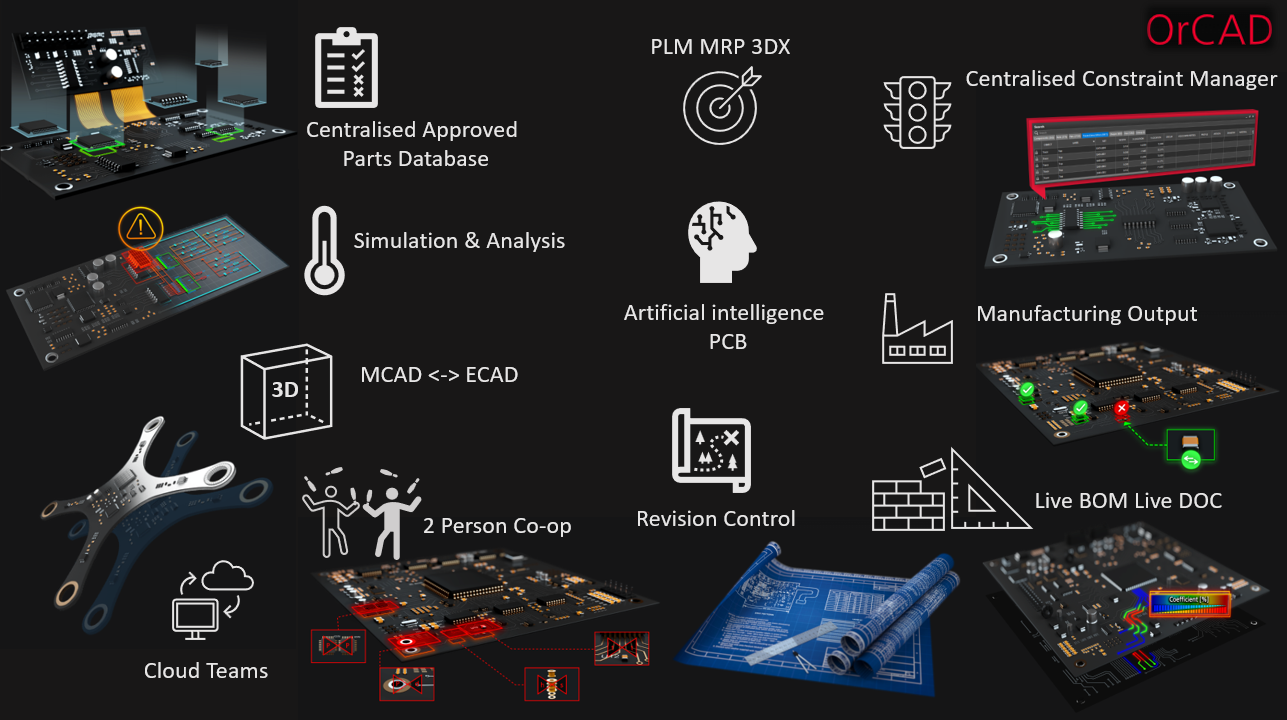
Please also view the PDF Presentation on what is new in OrCAD X and Allegro X here 
 

orcadxall